
Home » 行事
Category Archives: 行事
JST A-STEP 本格フェーズのプロジェクト開始
 JST A-STEP 本格フェーズのプロジェクトが採択されました。
我々はウエスタンデジタルテクノロジーズ合同会社と高機能トポロジカル量子材料の適用によるSOT-MRAMの実用化技術を2~3年で確立します。
エッジ、宇宙、量子コンピューターなど、低消費電力でAIを実行するためには、SRAM~DRAM並みの速度、書き換え回数1兆回以上、かつ埋め込みができる不揮発性メモリが必要です。我々は科学大で開発した独自な高機能トポロジカル量子材料を適用し、CMOSのBEOLに対応可能な400度以上のプロセス温度、1/10以上の低電流書き込み、バイアス磁界が不要なSOT-MRAMの実用化技術を開発します。
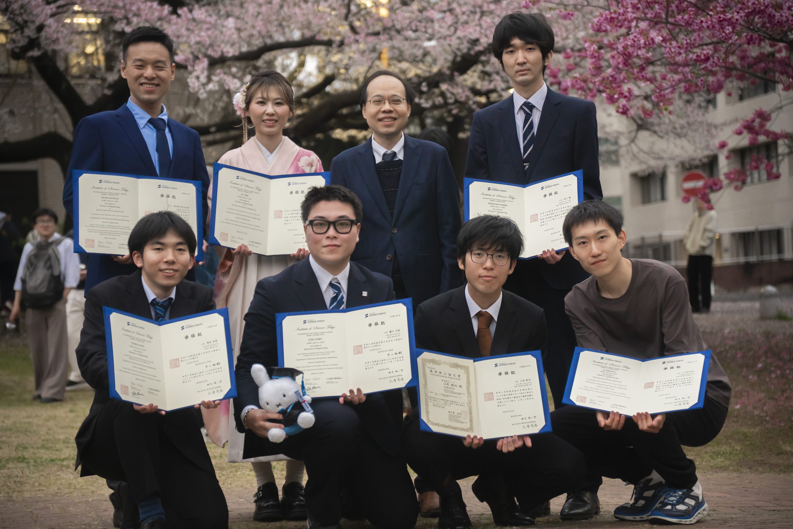
2025年度卒業式
2026年3月26日に2025年度の卒業式が行われました。博士課程の西山君、Zhang君、Liuさん、修士課程の江尻君、李君、石田君、学士課程の藤江君、連尾君、顔君が無事に卒業しました。おめでとうございます!
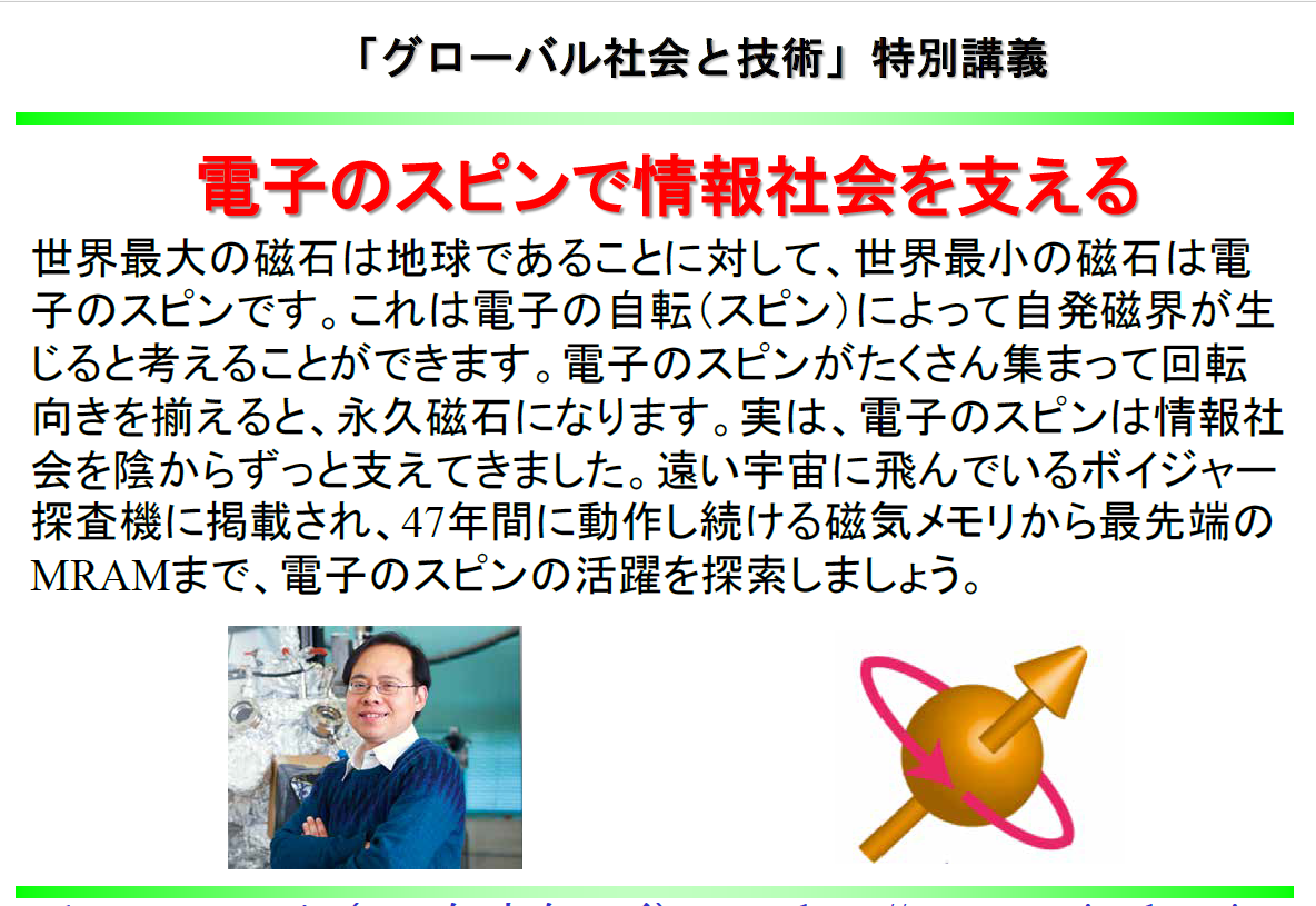
付属高校での特別講義
Pham教授は科学大付属高校で「グローバル社会と技術」特別講義を行いました。
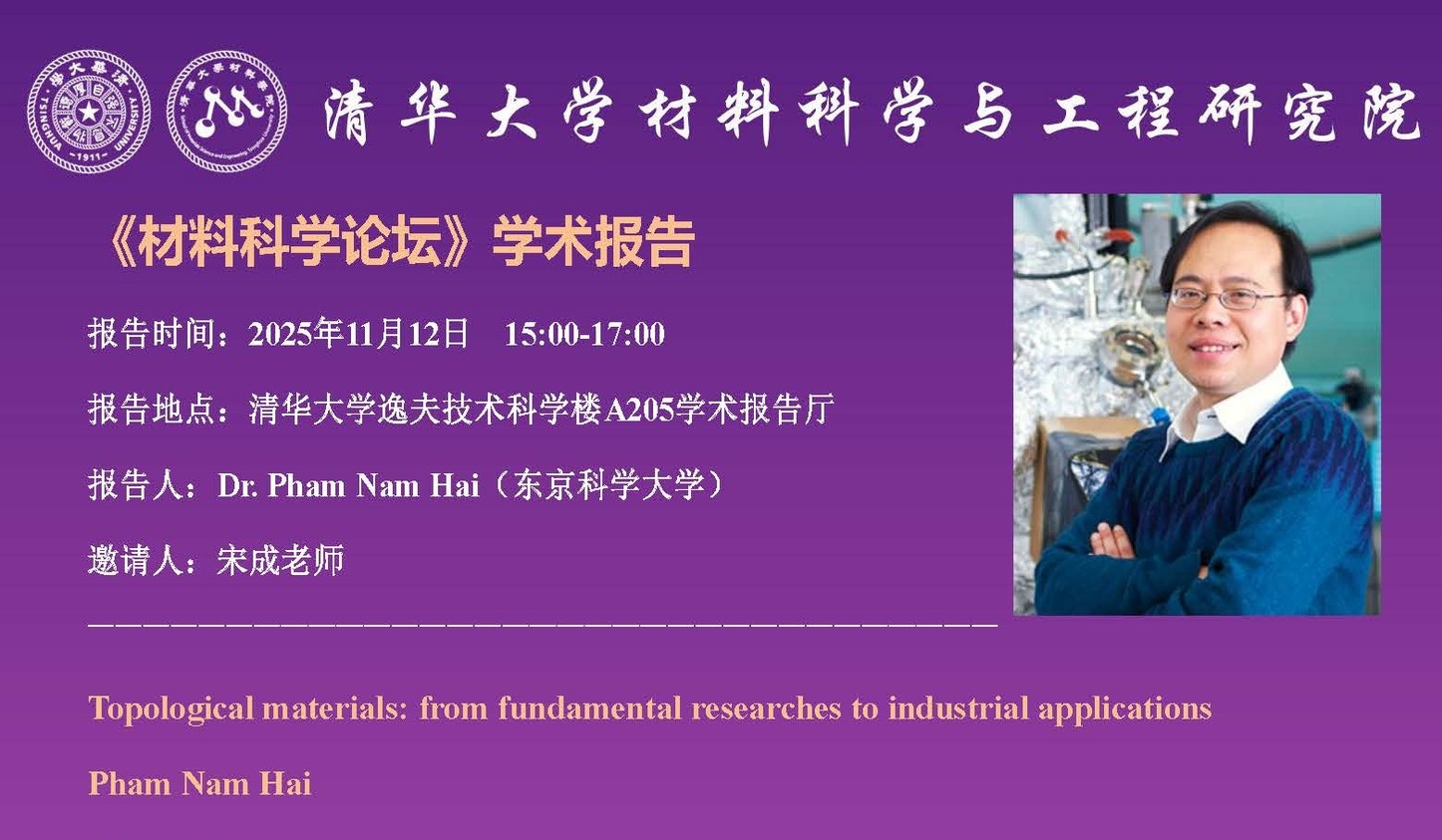
清華大学でのセミナー講演
Pham教授は中国の清華大学材料学科で下記のセミナー講演を行いました。
R7年度の新しいメンバー
新B4の連尾君、藤江君(B2D)、顔君、東京電機大学から新M1の籠君、ホーチミン市教育大学から新M1のTrinh Dai Hoang Long君、北陸先端科学技術大学院大学から新D1のPham Van Thuan君が研究室に加えました。また、大枝君と伊藤君がM1に、加々美君がD1に進学しました。また、Ho Hoang Huyさんが助教に着任しました。皆さんの活躍を期待します。
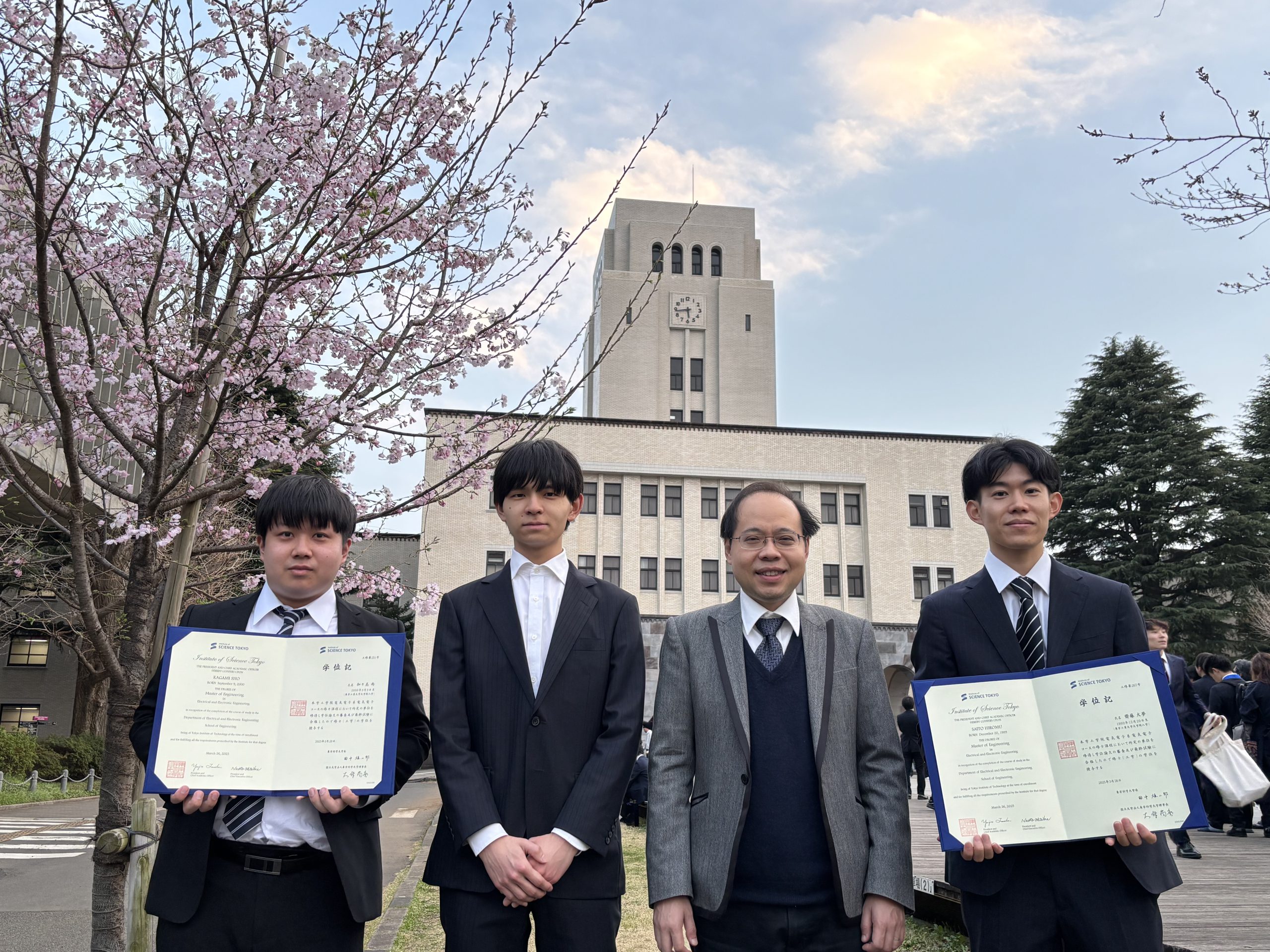
R6年度卒業式と送別会
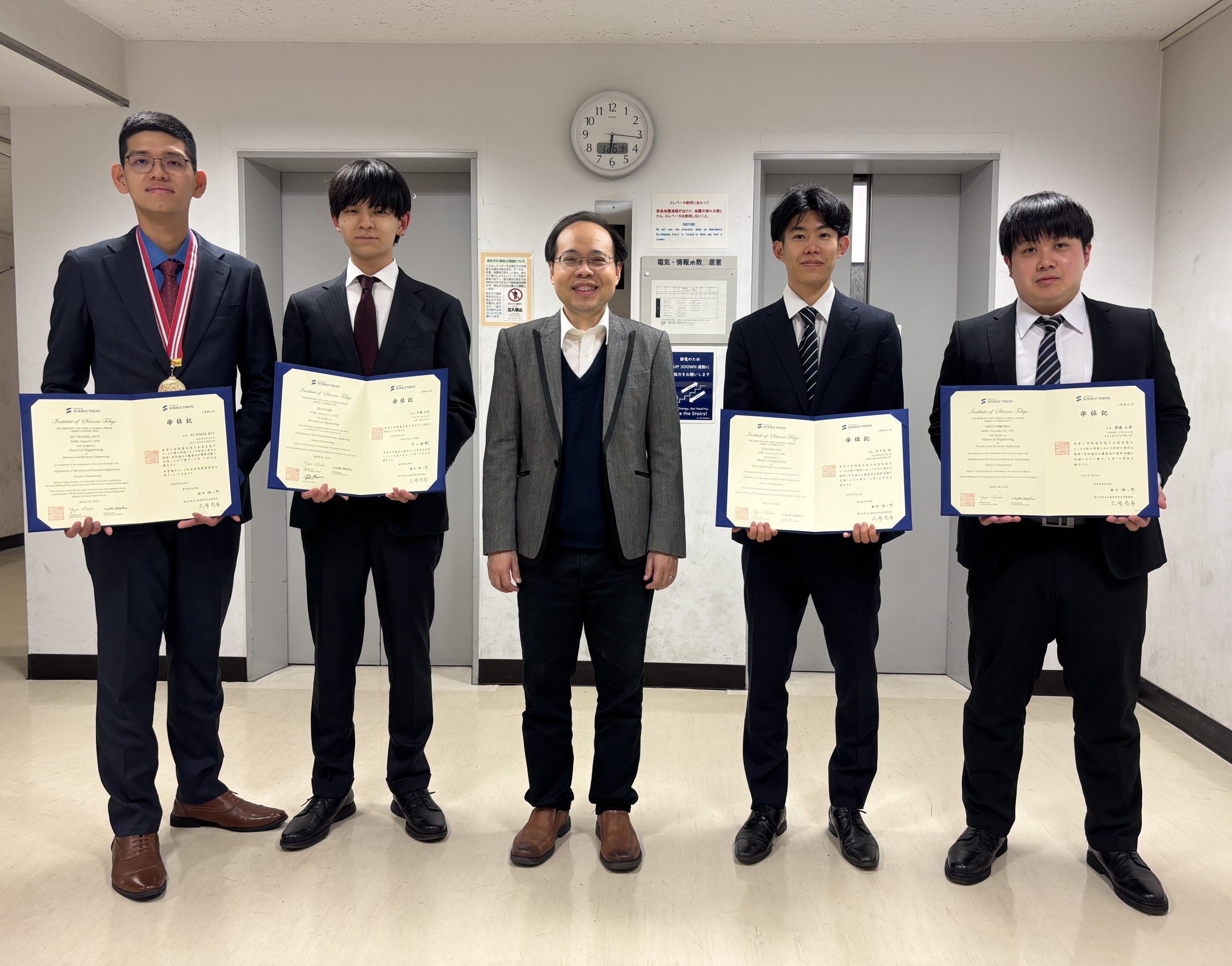
3月2 6日に、初春の桜が咲く晴天の中、R6年度の卒業式と送別会が行われました。B4の大枝君と伊藤君、M2の加々美君と齋藤君、D3のHuy君が無事に卒業しました。また、加々美君は優秀修士論文賞を受賞し、Huy君は電気電子系電気電子コースおよび超スマート社会卓越教育院の令和7年3月博士課程修了者の代表に選出されました。おめでとうございます!
海外訪問学生の研究室参加
中国の南京大学から3年生のMa Minzhe (马敏喆)君が海外訪問学生として研究室に参加しました。
新しいメンバー
新B4の伊藤君と大枝君、北海道大学から新M1の佐藤君、韓国の大学から新D1のHu YiFan君が研究室に加えました。また、江尻君、石田君と李君がM1に進学しました。皆さんの活躍を期待します。
R5年度の卒業式と送別会
3月26日に、冷たい雨の中、R5年度の卒業式と送別会が行われました。B4の江尻君と石田君、M2の長田君、高林君、南波君、山本君が無事に卒業しました。また、江尻君と石田君が電気電子系学士優秀学生賞の表彰を受けました。おめでとうございます!
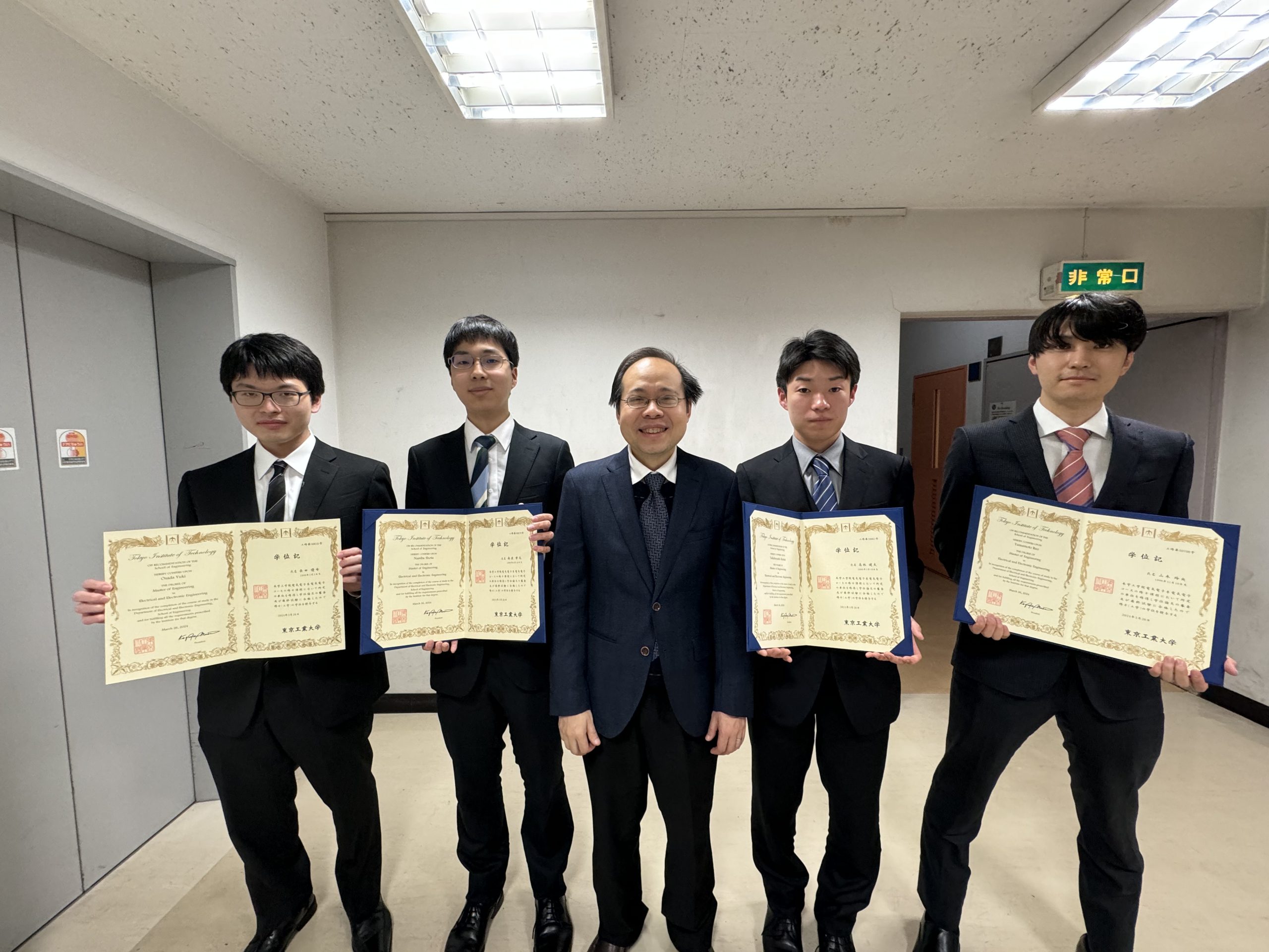
修士の皆さん
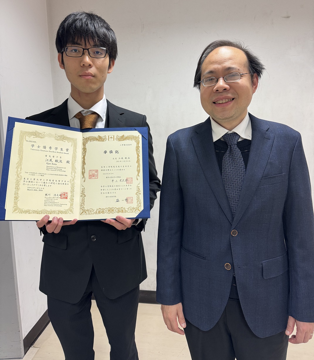
電気電子系学士優秀学生賞を受賞したB4の江尻君
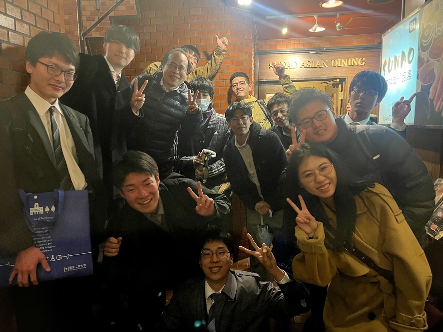
みんなで飲もう!
トポロジカル量子ビットに関するセミナーのご案内(11月24日(金)の13H30から)
Microsoft社や欧米の研究機関で活発に開発を進めているノイズ耐性があるトポロジカル量子ビットに関するセミナーをご案内します。
時間:11月24日(金)の13H30~
場所:南3号館第1会議室(S3-201号室)
講師:Dr. Tobias Schmitt (Forschungszentrum Jülich)
Title:
Versatility of selective area growth and stencil lithography for topological insulator-superconductor hybrid devices
Abstract:
As a potential platform to realize elusive topological superconductivity, hybrid devices of topological insulators (TIs) and conventional s-wave superconductors (S) form an attractive field of research. However, the fabrication of pristine hybrid devices with transparent S-TI interfaces is often hampered by degradation at ambient conditions. As a possible solution to this challenge, a novel technique combining selective area growth and stencil lithography to fabricate these devices under ultra-high vacuum (UHV) conditions has recently been reported. In my talk, I will showcase the versatility of this UHV fabrication technique for the implementation of several S-TI hybrid devices, ranging from Josephson junctions to superconducting hybrid qubits, and discuss their characterization.